Using old school split flap display as modern clock
What is it
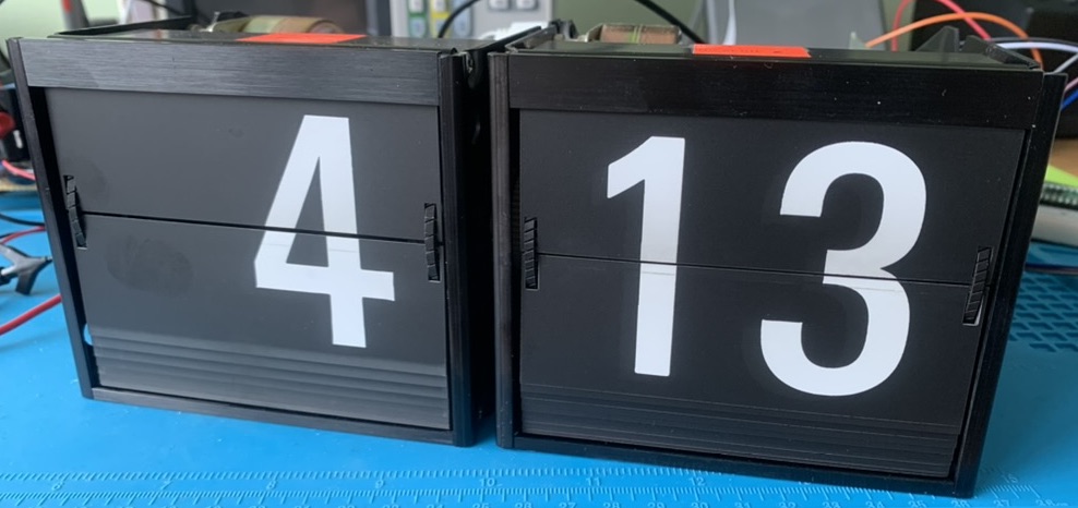
Everyone knows the split flap display from old airports or train stations and the natural “flapping” sound they make when being operated. These display have long been replaced by modern ones using LCD or even TFT monitors. Some of the newer modules emulate the sound of the real mechanical displays since we’re so used to the sound.
I grabbed two display on ebay, one with 0..23 and one with 0..60, with the idea to create a nice clock. Getting the modules and the documentation led to long nights of trying to understand how these modules work…but see below.
What else
Since the Raspberry RP2040 was recently released and available and cheap, I wanted to use this ARM processor in form of a Raspberry Pico board. It is just 4€ for a two core Cortex-M0 with a nice SDK and even a (more or less) build in hardware debugger.
In addition the clock should have DCF77, so being a radio controlled clock, illumination of the digits, measurement of temperature and humidity and a nice display in addition to the mechanical ones.
Standard hardware setup
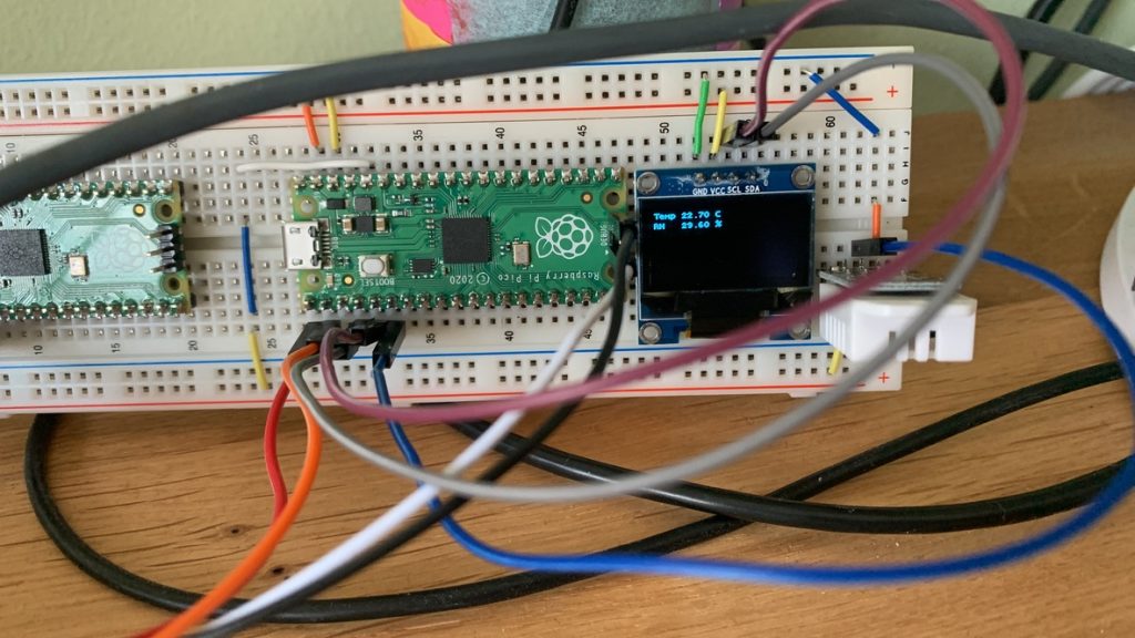
I used DCF77 receiver from ELV, A DHT22 module from joy-it and a 128×64 OLED display also from joy-it. This all was tied to the RP2040’s GPIO pins with a bit of glue hardware – no big deal. The real magic is the split flap display connection and – surprisingly – the DCF77 module.
DCF77 modules are a pain
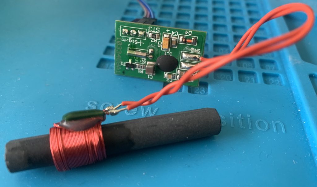
First I used a DCF module from Polin Electronics (cheap), but I was not able to convince it to really receive a clear signal. I tried every tip you can Google but nothing helped reliably.
So I bough a new one from ELV (double price) – this was a major improvement, but still not as good as possible. So I poked around with some filtering stuff in the power supply and the input signal until it worked at least “more often”.
The DCF receivers seem to be very picky with the power supply – cheap USB power supplies lead to no signal immediately. Connecting the RP2040 to my mac’s USB worked best on the bench – obviously the filtering is quite good here. See the schematic for an idea of the circuit.
The Split Flap (Fallblatt) Modules
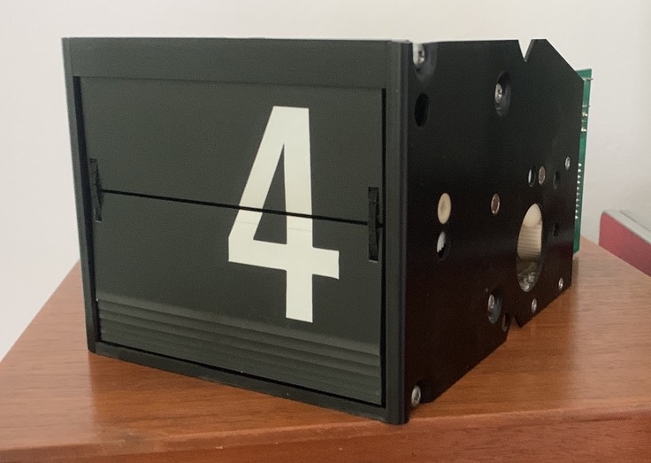
I got OMEGA 3021 modules which are far more complicated than the ones from other manufacturers. The control circuit on the board is really fine 80-ties tech, which took me hours to understand why they made it so complicated.
Before digging into this, please take a look at the original documentation (which I copied to my github project) – there is also a translation of the French description of the timing diagram.
How do the modules work
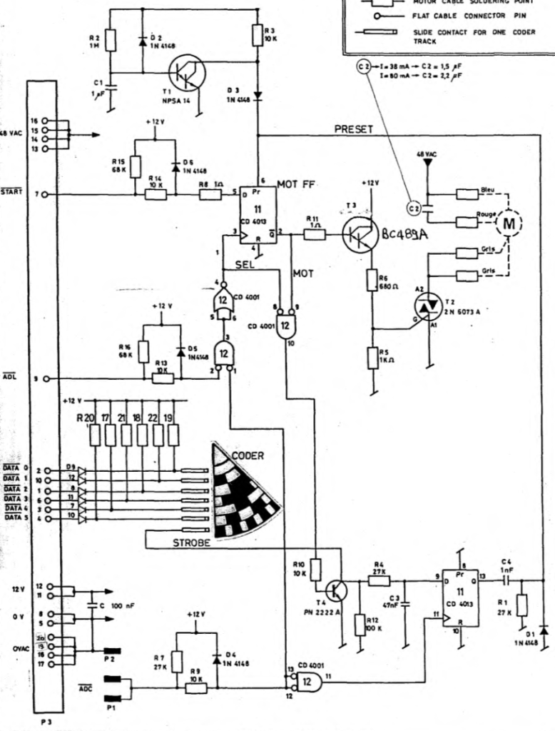
Every module has a /ADL and /ADC selection signal together with a /START signal whether it should spin the motor or not. L stands for line and C stands for column, meaning that the display elements are designed to be operated in a matrix.
If both /ADL and /ADC of a display are low, the display is selected. Once you “unselect” it (by raising /ADL or /ADC) it looks at the /START signal. If it is low, the motor starts – if it is high the motor does not start.
The position of an individual module is provided by an encoder. The display logic puts the encoder values (all low active) on the encoder bus when a display element is selected (/ADL and /ADC is low) and when the motor is stopped. Otherwise it will always be 111111, so all digits inactive.
The encoder bus is one reason for the complicated schematic. In fact it forms a data bus, so that you can connect all /DATAx lines of all display to the bus – less uP pins needed.
And how (and when) does the motor stop? Again some tricky trick. The uP signals the display element to stop the motor if it is on a valid flap position by lowering /ADC. If it is not in a valid position, the motor will continue to run. Please note, that a low edge on /ADC is enough. Again think about the matrix (see below) – this means all display elements of one column will get this trigger at once!
You can determine if an individual element reached a valid position by lowering /ADL (thus selecting it) and if the motor has stopped (because it reached a valid position) you will be able to read the encoder value. When you then release /ADL again, the module will take a look at /START – see above.
And why did they make it so complicated? Imagine some timing:
- A display full round takes six seconds
- The “strobe ticks” on the encoder are about 0.75mm, the encoder diameter is about 43mm, means the circumference is 270mm
- The speed at the outer track (where strobe is) is about 45mm/s
- This means the strobe pulse will have a “contact time” of around 17ms
So if you want the uP to really stop at a valid position, you will have to poll much more often than 17ms, let’s say every 1,7ms. This is no issue with one or two display elements, but imagine you have 1024. This would give you 1,7us per module and this is much shorter than the RC-anti-bounce delay (and the uP will be quite busy polling).
By the start/stop logic, the module automatically stops at a valid position once the uP signalled it to do so (by lowering /ADC), relaxing the timing significantly. Why? Because the lowest duration of a single “flap” is 100ms (6 seconds / 60 digits) – quite different than 1,7 ms.
The matrix
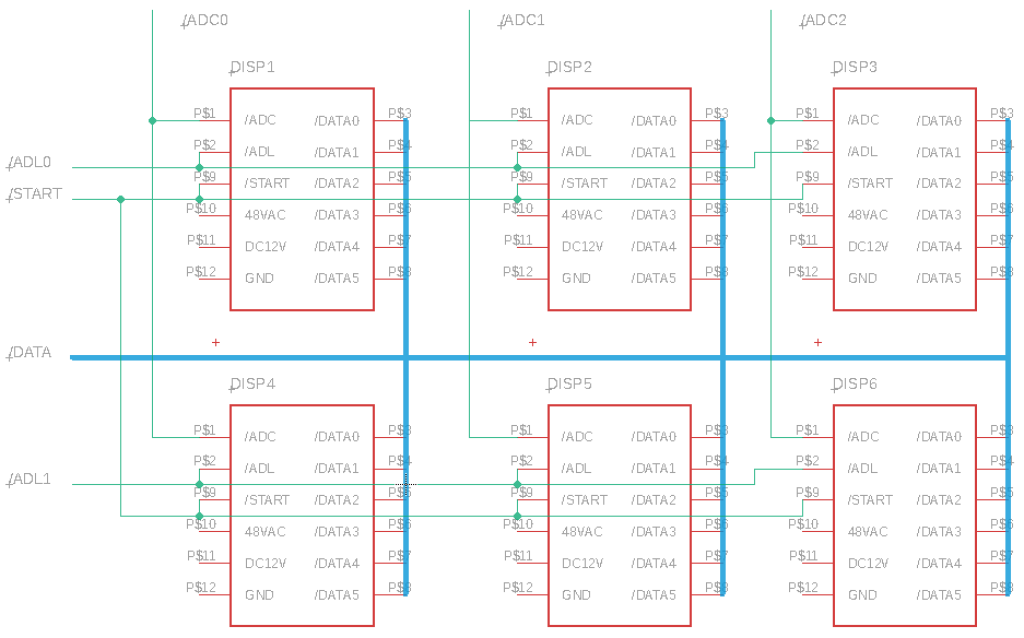
So let’s take a look at the matrix. All /ADCs of a column are connected (that’s why they are not on the flat cable bus), the /ADLs of a line are connected via the flatbed cable (on the bus), the /START signal of all display elements can be connected as well as all /DATAx lines. By creating a fancy multiplexed /ADLx and /ADCy circuit you can reduce the number of GPIOs significantly.
Let’s assume we have an average airport display. We use 16 lines and each line has 64 characters. This gives us 1024 display elements. To encode the 16 /ADLs, we need 4 bit, to encode the 64 /ADCs we need 6 bit. So with 4 (/ADLx) + 6 (ADCx) + 1 (/START) + 6 (/DATAx) = 17 GPIOs we can control 1024 display elements.
Not too bad – good Swiss engineering.
Crazy stuff
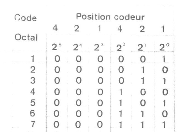
You might wonder why the Omega engineers selected this seldom octal code for the encoder. The reason for this is, that at any time at least one bit of the encoder has to be high on a valid flap position to flow through the Strobe line and switch input D of FFP2 to high because that is the internal motor stop signal. When selecting the display element though, strobe is connected to GND via T4 and is putting the encoder value on the bus.
Powering the module
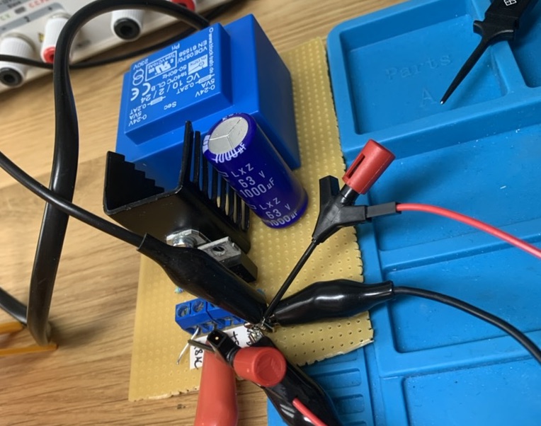
The module needs 12V and 48V AC, but the “cold” side of the 48V AC has to be connected to ground to make the T2 circuit work. This implicates some design challenges for the power board if you just want to use only one transformer (not a big deal with the 1024er display with I guess many transformers).
See below for a discussion.
Power Supply

Since we need an AC voltage, an external power supply was not an option. An integrated one is needed. For the other parts of the clock, we need also +5V DC, so in total we need three voltages.
Transformer
To get 48V AC, you cannot use a 48V or 2x24V transformer since the open circuit voltage is typically 20% above the nominal voltage and the motor in the display module is specified to tolerate only +10%/-15%. So I used a 24V AC transformer, giving us around 24V-30V AC – this is enough to power the motor.
Rectifier
Since we need to connect one end of the secondary coil to ground, we cannot use a bridge rectifier. Instead we use a simple diode and a much bigger sieve cap to compensate.
Be aware of the DC voltage: it goes easily to 41V DC.
Line regulation
As you can see in the schematics above, 12V are generated using a LM317T. This has been selected since it is a floating regulator only limited by the voltage difference of Vin and Vout. A 7812 for example has a max Vin of 40V so would probably die.
This is also the reason for having the 7805 for the +5V in series to the LM317T – by this it only has to cater for the 12V input voltage.
Cooling
The LM317T needs a heatsink for the 150 mA it should provide. It has to cover P = (24V * 1, 2* 1,41 – 12V) * 0,150A => 4,3W. Using a 10 C/W heatsink the maximum junction temperature will be t = 4,3W * (0,5 C/W + 5 C/W + 10 C/W) + 50 °C => 116 °C which is below the specified 125 °C. The 0,5 are from the thermal paste, the 5 from the LM317 specs and the 10 are the heatsink. 50 °C is the assumed maximum ambient temperature.
The 7805 does not need one. Assuming also 150 mA: P = (12V-5V)*0,150A => 1,05W. So t = 1,05W * 50 C/W + 50 °C = 102,5 °C.
Control Board
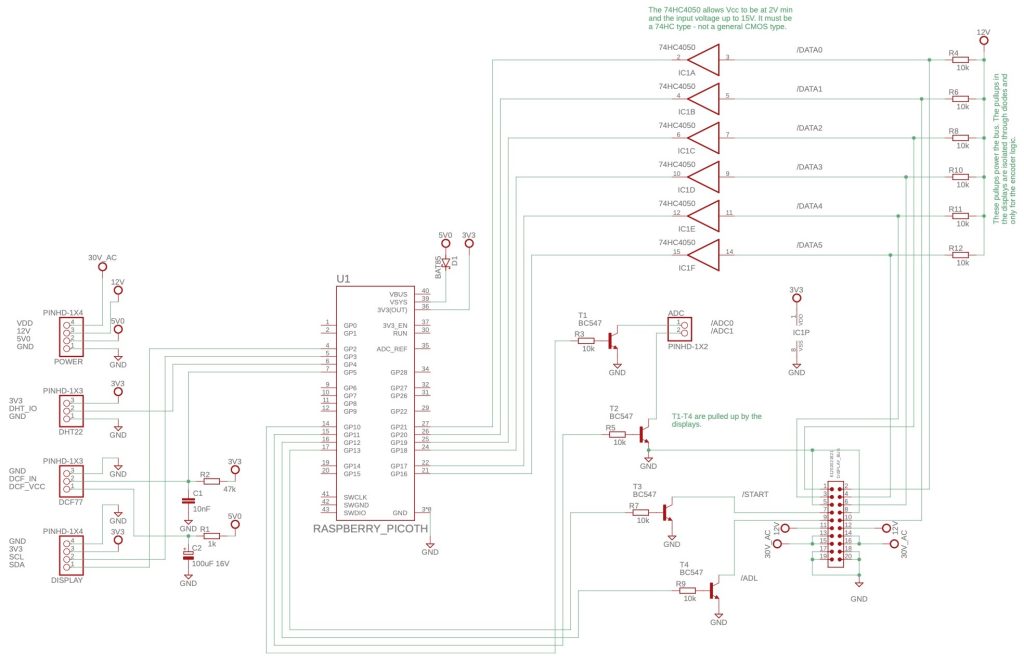
The control board is putting it all together. On the left hand side you see the very standard connections of the DCF77 module, the DHT22 sensor and the OLED display. The only special thing are the DCF_IN filter and the DCF_VCC filter.
On the right hand side the you see the display module interface. The output signals get transformed from 3.3V level to the 12V level of the display elements. The necessary pull-ups are on the display element boards. The signals are inverted by the circuit.
The input signals are transformed using a 74HC4050. The pull-up resistors are necessary to power the bus lines – the pull-ups on the displays are isolated using diodes. Please note, that here no inverting takes place.
My two displays are used as “one line” and “two columns”, so there are two /ADC lines, one for each display.
What’s next?
In the next blog entry, we will take a look at the software. It includes general purpose classes for driving the display elements in a flexible arrangement and a DCF77 library since it did not find a suitable one for the RP2040
